WMSIC Electronic Components

ADI/LINEAR MAX4372TEUK+T MAX4372TEUK

ModelMAX4372TEUK+T
PackageSOT-23-5
BrandADI/LINEAR
Price Price on request Electronic component prices change quickly with market supply and demand. Please refer to the latest WMSIC quotation for current pricing.
Configuration
1 options
Configuration 24+

Available for RFQ

Technical data

Product details

19 specifications

Core information

Product name
ADI(Analog Devices) / LINEAR MAX4372TEUK+T
Type
ADI/LINEAR
Minimum package
2500 圆盘

Technical parameters

Electronic Component
ADI(Analog Devices) / LINEAR
Electronic Component
MAX4372TEUK+T
Electronic Component
20V/V
Electronic Component
1
Package
SOT-23-5
Electronic Component
275kHz
Electronic Component
Current Sense Amplifier
Electronic Component
0.043g
Electronic Component
1
Common Mode Voltage
0V~28V
Features
Shunt; Analog Output Interface
Electronic Component
BM0258873071
Operating Temperature
40℃~+85℃
Voltage
±0.3V
Amplifier
1

For datasheets, package documents, compatible-part guidance, or other technical resources, contact WMSIC customer service. Availability is confirmed case by case.

MAX4372TEUK+T 产品概述

一、概述

MAX4372TEUK+T 是一款面向高压侧电流检测的微功耗电流检测放大器(current-sense amplifier),适合高侧电流监测及电流采样场合。器件采用 SOT-23-5 小封装,工作于单电源 2.7V 至 28V,并能在高达 28V 的共模电压下对负载电流对应的分流电阻两端差分电压进行 20V/V 的放大输出。器件静态电流仅约 30µA,输入偏置电流低(约 1µA),输入失调电压小(约 300µV),非常适合电池供电和低功耗系统中的长时间电流监测。

二、主要特性

  • 单路电流检测放大器
  • 共模电压范围:0V ~ 28V(高压侧测量支持)
  • 增益:20 V/V(固定)
  • 带宽(小信号增益带宽):约 275 kHz
  • 差分输入电压范围:-0.3V ~ +0.3V
  • 输入失调电压 (Vos):约 300µV
  • 输入偏置电流 (Ib):约 1µA
  • 共模抑制比(CMRR):≈ 85 dB
  • 单电源工作电压:2.7V ~ 28V(最大电源差 VDD–VSS = 28V)
  • 静态电流(Iq):约 30µA(微功耗特性)
  • 工作温度:-40℃ ~ +85℃
  • 封装:SOT-23-5(小型封装,带盘带卷供货,+T 表示卷带包装)

三、典型电气性能摘要(基于规格)

  • 输出电压与差分输入关系:VOUT ≈ Gain × (VIN+ − VIN−) = 20 × VDIFF
  • 对应的最大差分输出幅度(在允许的差分输入±0.3V 情况下):约 ±6V(实际输出受电源电压和输出摆幅限制)
  • 小信号带宽约 275kHz,适合较低频率的电流波形采样和峰值检测
  • CMRR 85 dB,能有效抑制高共模电压下的干扰

四、引脚与封装(示意)

典型 SOT-23-5 引脚分配(请以具体器件数据手册为准):

  • IN+:差分输入正端(接分流电阻高侧或低侧一端)
  • IN−:差分输入负端(接分流电阻另一端)
  • V+(VDD):供电正极(2.7V ~ 28V)
  • GND:地
  • OUT:放大器输出(对外提供与差分输入成比例的电压)

注:实际引脚排列请参照官方规格书和封装图。

五、典型应用场景

  • 高侧电流监测(电源管理、功率监控)
  • 电池管理系统(BMS)中的充放电电流测量
  • 过流检测与保护电路
  • 电机驱动与功率转换器中的电流采样
  • 通信与工业设备中低功耗电流监测

六、设计与使用注意事项

  • 差分输入限制:差分电压不得超过 ±0.3V,否则可能导致器件损伤或失真。因此分流电阻和最大测量电流需匹配,确保 Vshunt = I × Rshunt ≤ 0.3V。
  • 放大倍数关系:输出电压 VOUT = 20 × Vshunt。在设计时需保证 VOUT 在供电电压范围内并留有足够的摆幅裕度。例如:若希望输出不超过 5V,Vshunt 最大约为 0.25V(即 I × Rshunt ≤ 0.25V)。
  • 失调与输出误差:输入失调 300µV 放大后约为 6mV 的输出偏差(20×300µV),对大多数测量场合影响较小,但在高精度需求时需校准或补偿。
  • 输入偏置电流产生的误差:1µA 的输入偏置电流在高阻抗源上会产生额外电压降,应在分流电阻和接线电阻选择时考虑该项误差。
  • 带宽与脉冲测量:275kHz 的带宽适合测量较低频率和中等速度的电流变化,但对于非常窄脉冲或高频纹波,需要注意增益下降与相位延迟。
  • 布线与滤波:为降低共模干扰和高频噪声,建议将差分输入的走线靠近并尽量短,必要时可在输入端并联小电容形成 RC 滤波,但需保证差分电压限制内且滤波电容不会影响共模工作点。
  • 熱与封装:SOT-23-5 为小功率封装,长期大电流导致分流电阻发热可能影响测量精度,应关注热设计与散热路径。

七、示例计算

假设希望测量最大 1A 电流,要求放大器输出满量程约 2V,则所需分流电阻: Vshunt_max = 2V / 20 = 0.1V → Rshunt = 0.1V / 1A = 0.1Ω 在此设计下,器件安全且输出位于常见 ADC 输入范围内,且满足差分电压小于 ±0.3V 的限制。

八、总结

MAX4372TEUK+T 是一款适合高压侧、低功耗场合的电流检测放大器,凭借 0–28V 的共模支持、20V/V 的固定增益、低静态电流和小失调,适用于电池供电系统、过流保护和工业电流监测等应用。在系统设计时注意差分输入限制、输出摆幅与分流电阻的配合,以及必要的布线与滤波措施,可实现稳定、准确的电流测量。有关精确引脚定义、电气特性曲线和典型应用电路,请参见官方数据手册以获得详细参数与建议。

Request for quote

Send RFQ

Use the form for single models, category sourcing, and multi-line BOM requirements.

Send your target model and quantity.

Product sourcing intelligence

Model, package, availability, and BOM fit reviewed before quotation.

WMSIC turns product data, package visuals, BOM context, and sourcing signals into practical RFQ notes for buyers.

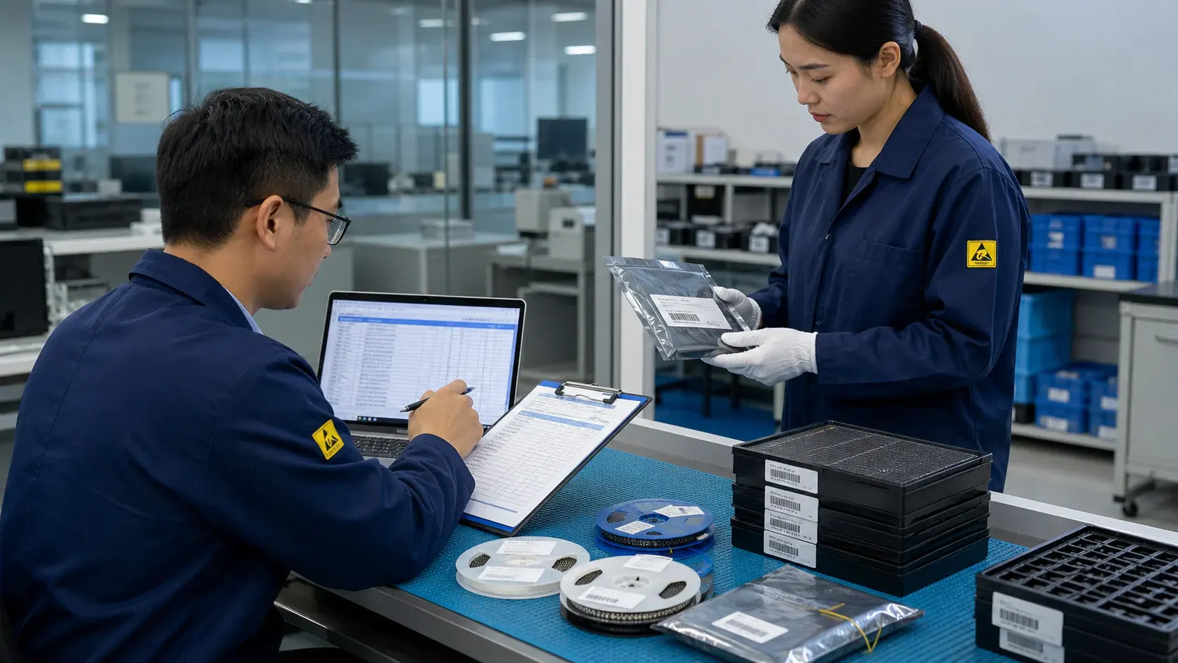
Electronic component model and package intelligence review on an ESD-safe inspection bench

Model & package intelligence

Model text, package form, tray or reel details, and visual evidence are reviewed together before RFQ feedback.

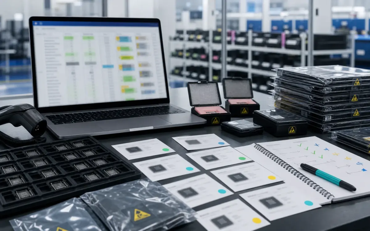
BOM matching and alternative component comparison workstation with protected IC samples

BOM matching & alternatives

BOM lines are compared by package, parameters, quantity, and workable alternatives for cleaner sourcing decisions.
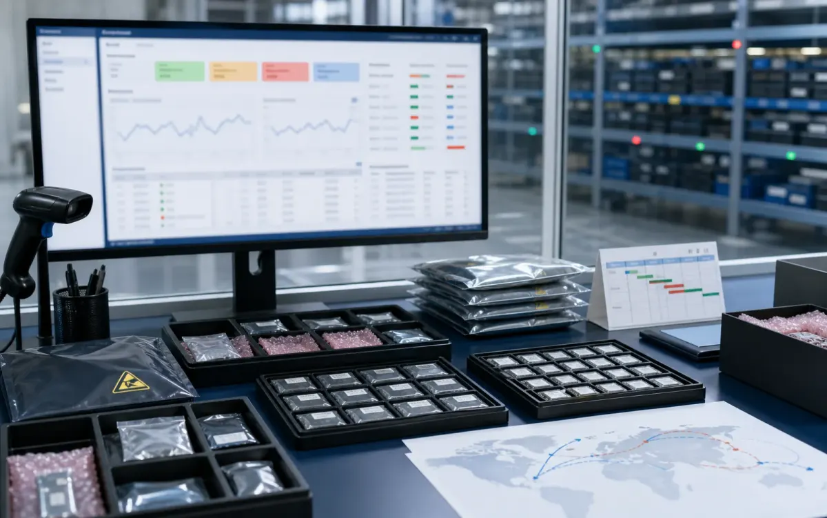
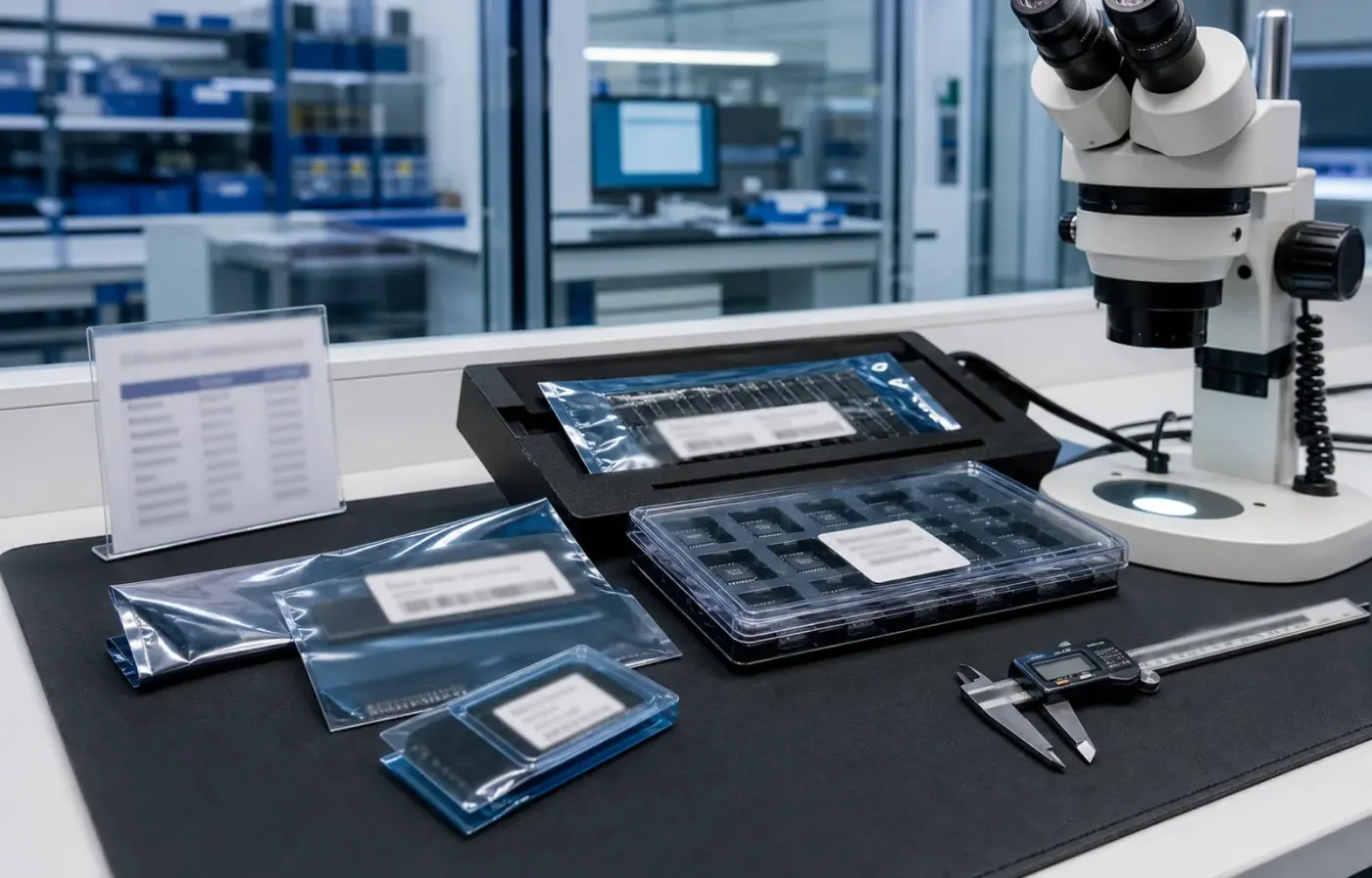
Electronic component sourcing availability dashboard with ESD-protected samples

Sourcing availability signal

Stock routes, quotation confidence, lead-time notes, and shipment feasibility are checked before sales follow-up.

Buyer sourcing scenarios

Examples of how common component sourcing requests are organized.

Typical RFQ scenarios based on the WMSIC form fields, catalog data, manual review steps, and shipment preparation workflow.

The buyer shares the full part number, package requirement, quantity, destination, and available product photos so the quotation can record the exact version under review.

Package confirmation Typical RFQ workflow

A multi-line BOM is organized into direct sourcing lines, lines that need package clarification, and lines where alternative-part review is permitted.

Mixed BOM triage Typical RFQ workflow

The original manufacturer part number, datasheet revision, application, critical limits, and acceptable changes are collected before possible candidates are discussed.

Obsolete-part review Typical RFQ workflow

Sample quantity, minimum packing, package format, target date, and courier destination are kept together in one RFQ conversation.

Small-batch request Typical RFQ workflow

Package photos, model markings, board context, and the quantity needed for repair help focus the sourcing review on the relevant version.

Repair batch evidence Typical RFQ workflow

When a suffix or package note is incomplete, the response records the open difference and requests buyer confirmation before procurement proceeds.

Model suffix clarification Typical RFQ workflow

Packing format, carton notes, invoice details, courier option, destination, and tracking handoff are coordinated around the confirmed order.

Export handoff Typical RFQ workflow

The request connects the previously used model, current demand, package evidence, target timing, and replenishment sourcing route.

Replenishment inquiry Typical RFQ workflow

Related products

Packaged components ready for RFQ.