
Model & package intelligence
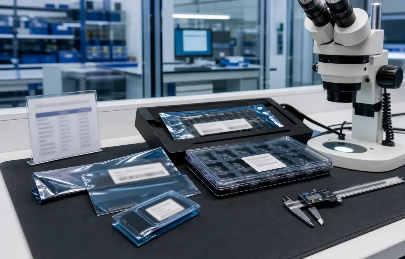
Model text, package form, tray or reel details, and visual evidence are reviewed together before RFQ feedback.
 WMSIC
Electronic Components
WMSIC
Electronic Components
Available for RFQ
Technical data
For datasheets, package documents, compatible-part guidance, or other technical resources, contact WMSIC customer service. Availability is confirmed case by case.
杭晶(HCI)CO53D6-156.250-33KDTSN是一款针对高速数字通信、工业控制及消费电子领域设计的工业级LVDS输出晶振。其156.25MHz基准频率为行业标准时钟源,精准适配千兆/万兆以太网、PCIe 2.0/3.0、高清视频传输等场景的核心芯片时钟需求,尤其适合对宽温稳定性、低噪声有要求的设备。
典型应用包括:
该晶振的核心参数围绕“高精度、低噪声、抗干扰”设计,具体如下:
采用低电压差分信号(LVDS)输出,优势显著:
典型相位噪声为:
采用SMD5032-6P小型化贴片封装,尺寸为5.0mm×3.2mm×1.2mm(长×宽×高),节省PCB空间,适合高密度设计设备。
符合IPC-J-STD-001标准,支持回流焊工艺(峰值温度260℃±5℃,时间≤10秒),适合自动化批量生产。
覆盖-40℃~+85℃工业级温度范围,可在严寒(如北方户外基站)或高温(如工业控制柜)环境下稳定运行。
杭晶对该产品进行了严格的可靠性验证:
符合RoHS 2.0及REACH标准,不含铅、镉等有害物质,满足全球市场环保要求。
需确认目标芯片的时钟输入频率是否为156.25MHz(如Intel I210千兆网卡、Broadcom BCM54680万兆PHY)。
LVDS输出需在接收端并联100Ω差分终端电阻(靠近接收芯片引脚),匹配传输线阻抗,减少信号反射。
晶振电源端建议串联10Ω~22Ω电阻,并联0.1μF陶瓷电容+10μF电解电容,过滤电源噪声。
该产品凭借杭晶的工业级制造工艺,在精度、稳定性及抗干扰性上均能满足中高端设备的时钟需求,是高速数字电路设计的可靠选择。
Request for quote
Use the form for single models, category sourcing, and multi-line BOM requirements.
Product sourcing intelligence
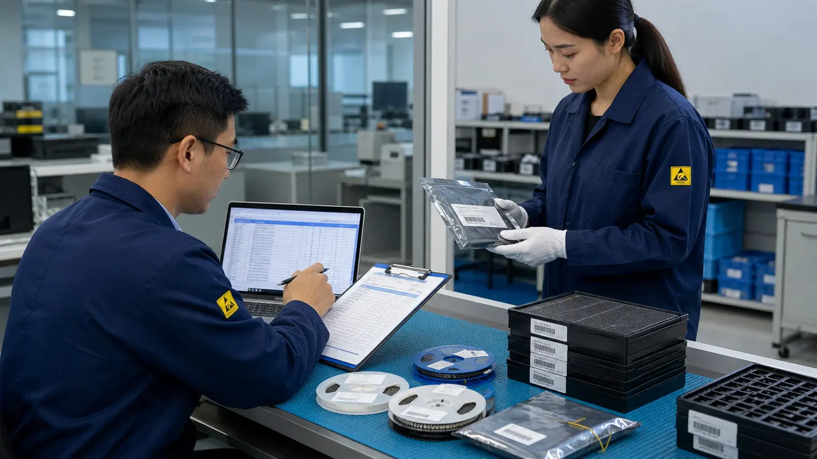
WMSIC turns product data, package visuals, BOM context, and sourcing signals into practical RFQ notes for buyers.
Model text, package form, tray or reel details, and visual evidence are reviewed together before RFQ feedback.
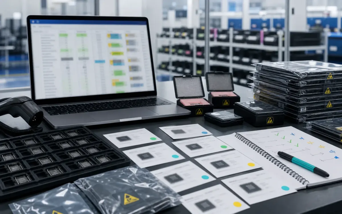
BOM lines are compared by package, parameters, quantity, and workable alternatives for cleaner sourcing decisions.
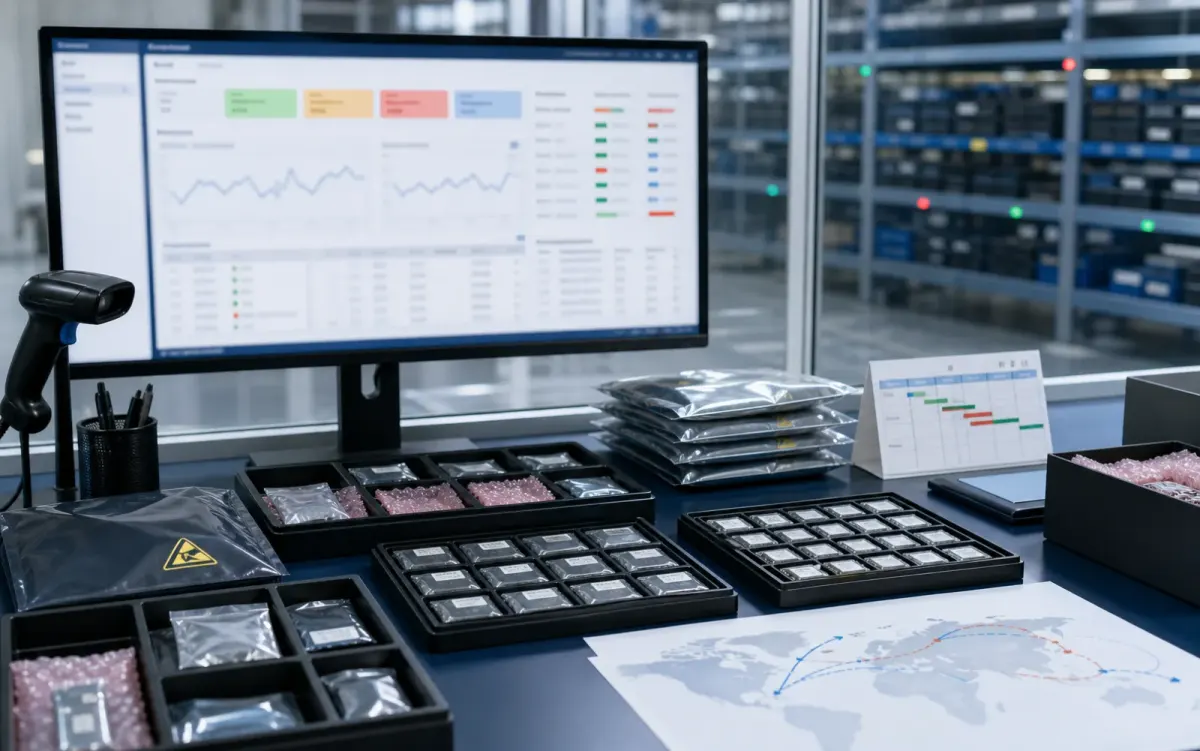
Stock routes, quotation confidence, lead-time notes, and shipment feasibility are checked before sales follow-up.
Buyer sourcing scenarios
Typical RFQ scenarios based on the WMSIC form fields, catalog data, manual review steps, and shipment preparation workflow.
The buyer shares the full part number, package requirement, quantity, destination, and available product photos so the quotation can record the exact version under review.
A multi-line BOM is organized into direct sourcing lines, lines that need package clarification, and lines where alternative-part review is permitted.
The original manufacturer part number, datasheet revision, application, critical limits, and acceptable changes are collected before possible candidates are discussed.
Sample quantity, minimum packing, package format, target date, and courier destination are kept together in one RFQ conversation.
Package photos, model markings, board context, and the quantity needed for repair help focus the sourcing review on the relevant version.
When a suffix or package note is incomplete, the response records the open difference and requests buyer confirmation before procurement proceeds.
Packing format, carton notes, invoice details, courier option, destination, and tracking handoff are coordinated around the confirmed order.
The request connects the previously used model, current demand, package evidence, target timing, and replenishment sourcing route.
Related products


