WMSIC Electronic Components

AOS AONS66406

ModelAONS66406
PackageDFN-8(5x6)
BrandAOS
Price Price on request Electronic component prices change quickly with market supply and demand. Please refer to the latest WMSIC quotation for current pricing.
Configuration
1 options
Configuration 26+

Available for RFQ

Technical data

Product details

20 specifications

Core information

Product name
AOS AONS66406
Type
AOS
Unit
Electronic Component
Minimum package
3000 圆盘

Technical parameters

Electronic Component
AOS
Electronic Component
AONS66406
Electronic Component
1
Package
DFN-8(5x6)
Electronic Component
1 N
Electronic Component
MOSFET
Electronic Component
0.202g
Electronic Component
1
Electronic Component
BM0227261989
Operating Temperature
55℃~+150℃
Electronic Component
3000
Voltage(Vdss)
40V
Capacitor(Ciss)
1.48nF

For datasheets, package documents, compatible-part guidance, or other technical resources, contact WMSIC customer service. Availability is confirmed case by case.

AONS66406 产品概述

一、概览

AONS66406 是 AOS(台湾宏晶)出品的一款高性能 N 沟道功率 MOSFET,额定漏源电压为 40V,额定连续漏极电流 30A,适用于中功率到高电流密度的开关电源与电源管理场景。器件采用 DFN-8 (5×6 mm) 小型封装,带裸露散热垫,便于通过 PCB 铜箔实现高效热管理。

主要电性能指标(典型/标称):

  • Vdss:40 V
  • Id(连续):30 A
  • RDS(on):6.1 mΩ @ Vgs = 10 V(在 30 A)
  • Vgs(th):1.5 V(门限电压)
  • Qg(总门极电荷):20 nC @ Vgs = 10 V
  • Ciss(输入电容):1.48 nF @ 20 V
  • Crss(反向传输电容):13 pF @ 20 V
  • 最高结温:-55 ℃ ~ +150 ℃
  • 封装:DFN-8 (5×6),额定功耗(示例):14.5 W(请参考具体数据手册中电源耗散与热阻规范)

二、关键特性与设计意义

  • 低导通电阻(6.1 mΩ @ 10 V):在高电流条件下导通损耗低,有利于减少发热与提升效率,适合作为同步整流管或高电流开关元件。
  • 合理的门极电荷(20 nC @10 V):门极驱动能耗适中,便于使用中等驱动能力的驱动器或 MCU 驱动器与专用门极驱动芯片配合,开关损耗与驱动功耗可在设计中权衡。
  • 较小的 Crss(13 pF):Miller 电容控制在较低水平,有利于减缓开关转换期间的耦合干扰与降低误触发风险,但在高 dv/dt 环境仍需注意门极布局与驱动策略。
  • 宽工作温度范围(-55~150 ℃):适应工业级环境及高温工作场景,但需配合良好散热设计保持结温低于规定上限。

三、典型应用场景

  • 同步降压(buck)转换器的高侧/低侧 MOSFET
  • 开关电源(SMPS)、DC-DC 转换模块
  • 电机驱动(中小功率)、负载开关
  • 电池管理与保护电路、逆变/UPS 系统的开关元件
  • 高密度电源管理板卡:需求小封装与较高电流承载

四、设计与布局建议

  • 门极驱动:推荐以 10 V 为参考驱动电压以获得标称 RDS(on)。若使用 5 V 驱动需校核导通电阻随 Vgs 的上升曲线,避免导通损耗显著增加。
  • 门极电路:为控制开关应力与抑制振铃,建议在门极与驱动之间并联 5–22 Ω 门极电阻,必要时在门极并联小阻值泄放电阻以防止浮空。
  • 热管理:利用 DFN-8 的裸露散热垫在 PCB 上设计充足的散热铜面积与过孔(thermal vias),按实际 PCB 铜量与空气对流条件计算结–外界热阻并验证结温(Tj)。器件额定连续电流与功耗值通常基于特定散热条件(如 Tc = 25 ℃),实际应用应做热仿真或测量验证。
  • 布局注意:将驱动器靠近 MOSFET 放置,减短门极回路路径;将感性开关节点(SW)走线最短,使用合适的旁路与去耦电容,避免大电流回路引入噪声到门极。

五、开关与损耗估算(实用示例)

  • 导通损耗估算:Pcond ≈ I^2·RDS(on)。例如在 30 A 时,Pcond ≈ 30^2 × 0.0061 ≈ 5.5 W(此为理想估算,实际应考虑温度导致的 RDS(on) 增大)。
  • 驱动能耗:Pgate ≈ Qg × Vdrive × fsw。以 Vdrive = 10 V、Qg = 20 nC、fsw = 500 kHz 为例,Pgate ≈ 20e-9 × 10 × 500e3 ≈ 0.1 W。该量级有助于选择合适门极驱动器并评估驱动损耗。

六、使用注意与可靠性

  • ESD 与静电敏感:MOSFET 对静电敏感,生产与焊接过程中应采取防静电措施(佩戴腕带、使用防静电垫等)。
  • 回流焊与湿敏:DFN 封装需要遵循厂商给出的回流焊曲线与潮湿敏感等级(MSL)说明,避免吸湿膨胀导致封装损伤。
  • 详见原厂数据手册:引脚定义、热阻参数(θJA/θJC)、SOA(安全工作区)和典型特性曲线请以 AOS 官方数据手册为准,芯片在不同工况下的电流与功耗能力依赖 PCB 散热设计与环境条件。

七、总结

AONS66406 在 40V/30A 级别上提供了低 RDS(on) 与中等门极电荷的平衡设计,适合对效率与体积有较高要求的电源应用。结合 DFN-8 的紧凑封装与良好 PCB 散热设计,该器件可在同步整流、开关电源与电源管理场景中实现优良的能效与热性能表现。选型与最终验证请参照 AOS 官方数据手册与 PCB 热设计规则完成全面评估。

Request for quote

Send RFQ

Use the form for single models, category sourcing, and multi-line BOM requirements.

Send your target model and quantity.

Product sourcing intelligence

Model, package, availability, and BOM fit reviewed before quotation.

WMSIC turns product data, package visuals, BOM context, and sourcing signals into practical RFQ notes for buyers.

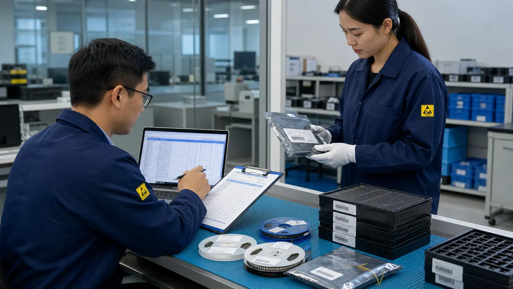
Electronic component model and package intelligence review on an ESD-safe inspection bench

Model & package intelligence

Model text, package form, tray or reel details, and visual evidence are reviewed together before RFQ feedback.

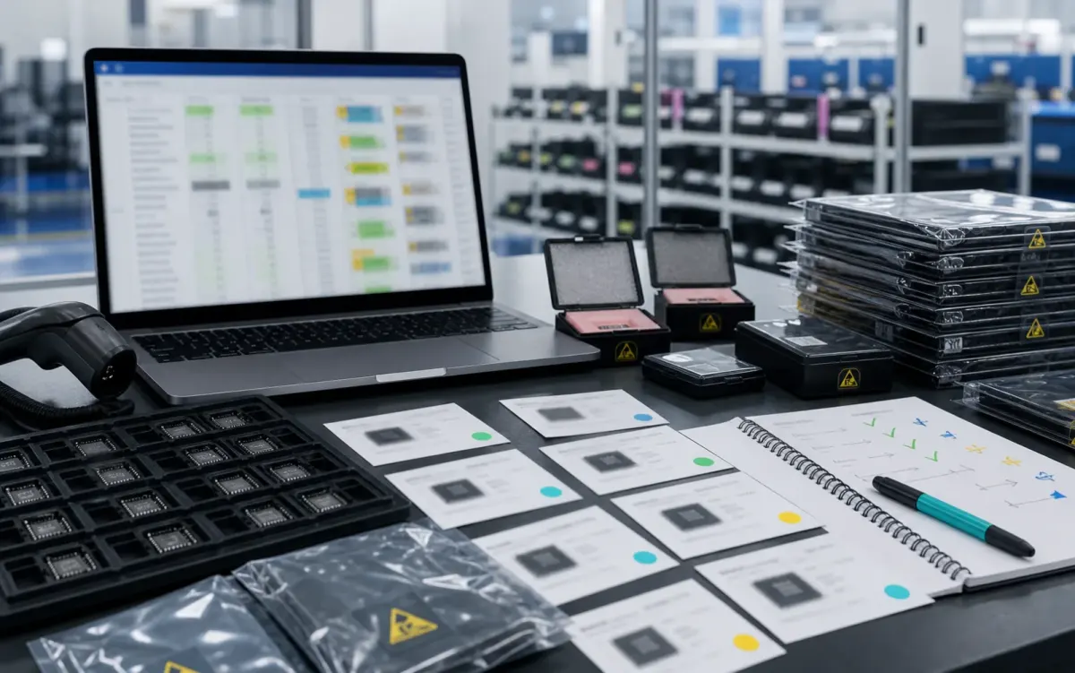
BOM matching and alternative component comparison workstation with protected IC samples

BOM matching & alternatives

BOM lines are compared by package, parameters, quantity, and workable alternatives for cleaner sourcing decisions.

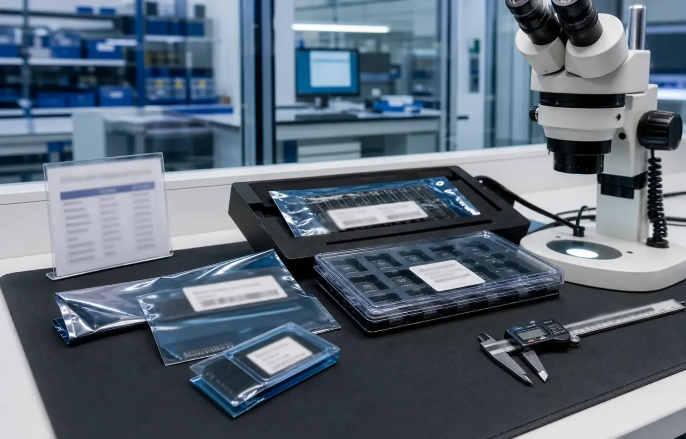
Electronic component sourcing availability dashboard with ESD-protected samples

Sourcing availability signal

Stock routes, quotation confidence, lead-time notes, and shipment feasibility are checked before sales follow-up.

Buyer sourcing scenarios

Examples of how common component sourcing requests are organized.

Typical RFQ scenarios based on the WMSIC form fields, catalog data, manual review steps, and shipment preparation workflow.

The buyer shares the full part number, package requirement, quantity, destination, and available product photos so the quotation can record the exact version under review.

Package confirmation Typical RFQ workflow

A multi-line BOM is organized into direct sourcing lines, lines that need package clarification, and lines where alternative-part review is permitted.

Mixed BOM triage Typical RFQ workflow

The original manufacturer part number, datasheet revision, application, critical limits, and acceptable changes are collected before possible candidates are discussed.

Obsolete-part review Typical RFQ workflow

Sample quantity, minimum packing, package format, target date, and courier destination are kept together in one RFQ conversation.

Small-batch request Typical RFQ workflow

Package photos, model markings, board context, and the quantity needed for repair help focus the sourcing review on the relevant version.

Repair batch evidence Typical RFQ workflow

When a suffix or package note is incomplete, the response records the open difference and requests buyer confirmation before procurement proceeds.

Model suffix clarification Typical RFQ workflow

Packing format, carton notes, invoice details, courier option, destination, and tracking handoff are coordinated around the confirmed order.

Export handoff Typical RFQ workflow

The request connects the previously used model, current demand, package evidence, target timing, and replenishment sourcing route.

Replenishment inquiry Typical RFQ workflow

Related products

Packaged components ready for RFQ.