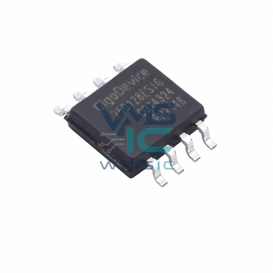
產品概覽
GD5F1GQ5REWIGR
SPI (Serial Peripheral Interface) NAND Flash provides an ultra-cost effective while high density non-volatile memory storage solution for embedded systems, based on an industry-standard NAND Flash memory core. It is an attractive alternative to SPI-NOR and standard parallel NAND Flash, with advanced features.\nTotal pin count is 8, including VCC and GND. Density is 1Gb. Superior write performance and cost per bit over SPI-NOR. Significant low cost than parallel NAND.\nThis low-pin-count NAND Flash memory follows the industry-standard serial peripheral interface, and always remains the same pin out from one density to another. The command sets resemble common SPI-NOR command sets, modified to handle NAND specific functions and added new features. It is an easy-to-integrate NAND Flash memory, with specified designed features to ease host management:。User-selectable internal ECC. ECC parity is generated internally during a page program operation. When a page is read to the cache register, the ECC parity is detected and corrects the errors when necessary. The 64-bytes spare area is available even when internal ECC enabled. The device outputs corrected data and returns an ECC error status.。Internal data move or copy back with internal ECC. The device can be easily refreshed and manage garbage collection task, without need of shift in and out of data.。Power on Read with internal ECC. The device will automatically read first page of first block to cache after power on, then host can directly read data from cache for easy boot. Also the data is promised correct by internal ECC when ECC enabled.\nIt is programmed and read in page-based operations, and erased in block-based operations. Data is transferred to or from the NAND Flash memory array, page by page, to a data register and a cache register. The cache register is closest to I/O control circuits and acts as a data buffer for the I/O data; the data register is closest to the memory array and acts as a data buffer for the NAND Flash memory array operation. The cache register functions as the buffer memory to enable page and random data READ/WRITE and copy back operations. These devices also use a SPI status register that reports the status of device operation.