
Model & package intelligence
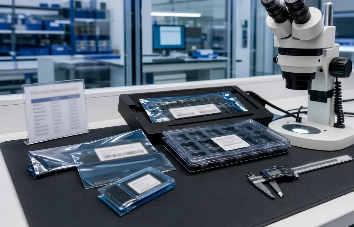
Model text, package form, tray or reel details, and visual evidence are reviewed together before RFQ feedback.
 WMSIC
Electronic Components
WMSIC
Electronic Components
Available for RFQ
Technical data
For datasheets, package documents, compatible-part guidance, or other technical resources, contact WMSIC customer service. Availability is confirmed case by case.
LM4041C12IDBZR是德州仪器(TI)推出的并联型固定电压基准芯片,专为低功耗、空间受限且对电压精度有基础要求的模拟电路设计。其核心功能是提供稳定的1.225V基准电压,广泛适配工业监测、便携设备、ADC/DAC参考等场景,凭借小封装、低静态电流等特性,成为中小精度模拟电路的常用选型。
该芯片的性能参数聚焦「精度稳定、功耗低、噪声小」三大核心,具体如下:
LM4041C12IDBZR采用SOT-23封装(3引脚),尺寸仅为1.6mm×1.0mm×0.8mm,大幅节省PCB空间,适合小型化设计。引脚定义如下:
需注意:并联基准的工作原理是「阴极电压比阳极高1.225V」,因此引脚连接时需确保阴极电位高于阳极。
该芯片的特性使其适用于以下常见场景:
1.225V固定输出可直接作为12位ADC的参考电压(如ADC的VREF引脚),低噪声特性保证转换精度;同时也可用于DAC的输出校准,提升模拟信号生成的准确性。
通过与比较器配合,1.225V基准可作为阈值电压,监测电源电压波动(如当电源电压低于1.225V时触发欠压报警),适用于电池供电设备的保护逻辑。
45μA静态电流可显著降低系统功耗,适合电池供电的便携设备(如手持万用表、无线传感器节点),延长电池续航时间。
宽温范围(-40℃~+85℃)可适应工业环境的温度变化,为温度传感器、压力传感器等的信号调理电路提供稳定基准,保证输出信号的一致性。
可作为BMS中单体电池电压监测的参考基准,配合运放放大电路,实现对电池电压的精准采样。
LM4041C12IDBZR凭借平衡的性能与成本优势,成为工业、便携等领域中小精度模拟电路的可靠基准选择。
Request for quote
Use the form for single models, category sourcing, and multi-line BOM requirements.
Product sourcing intelligence
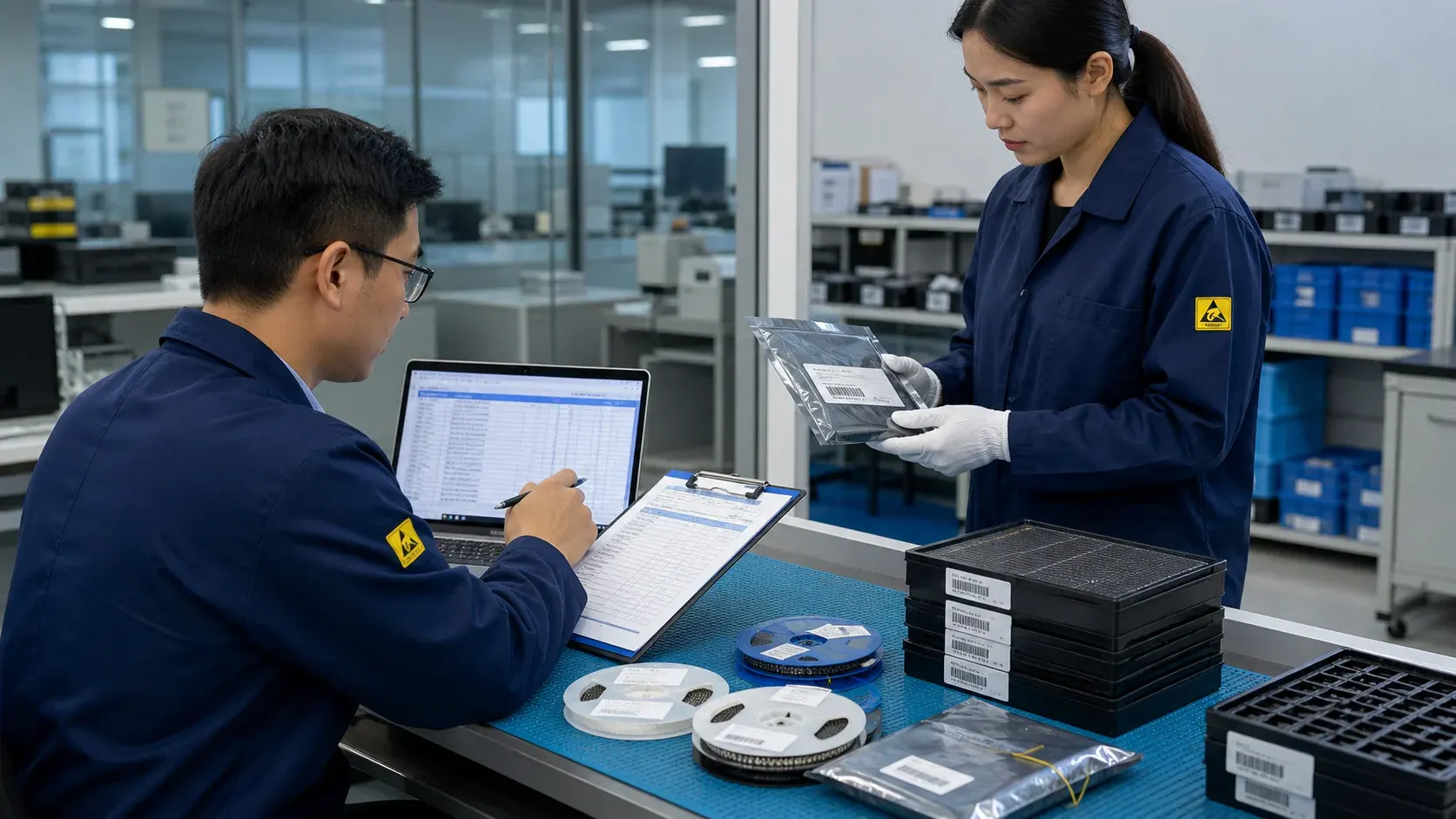
WMSIC turns product data, package visuals, BOM context, and sourcing signals into practical RFQ notes for buyers.
Model text, package form, tray or reel details, and visual evidence are reviewed together before RFQ feedback.
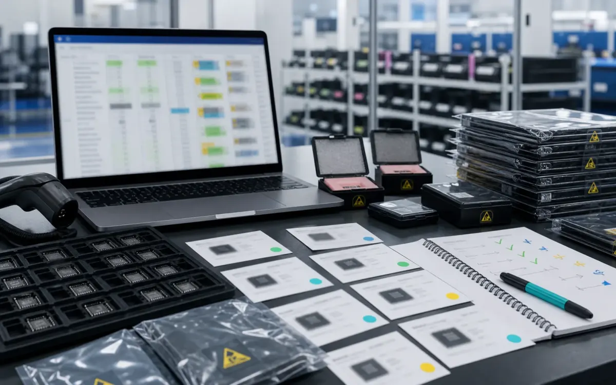
BOM lines are compared by package, parameters, quantity, and workable alternatives for cleaner sourcing decisions.
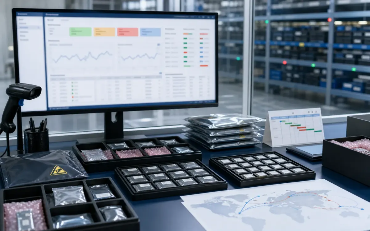
Stock routes, quotation confidence, lead-time notes, and shipment feasibility are checked before sales follow-up.
Buyer sourcing scenarios
Typical RFQ scenarios based on the WMSIC form fields, catalog data, manual review steps, and shipment preparation workflow.
The buyer shares the full part number, package requirement, quantity, destination, and available product photos so the quotation can record the exact version under review.
A multi-line BOM is organized into direct sourcing lines, lines that need package clarification, and lines where alternative-part review is permitted.
The original manufacturer part number, datasheet revision, application, critical limits, and acceptable changes are collected before possible candidates are discussed.
Sample quantity, minimum packing, package format, target date, and courier destination are kept together in one RFQ conversation.
Package photos, model markings, board context, and the quantity needed for repair help focus the sourcing review on the relevant version.
When a suffix or package note is incomplete, the response records the open difference and requests buyer confirmation before procurement proceeds.
Packing format, carton notes, invoice details, courier option, destination, and tracking handoff are coordinated around the confirmed order.
The request connects the previously used model, current demand, package evidence, target timing, and replenishment sourcing route.
Related products


