Model & package intelligence
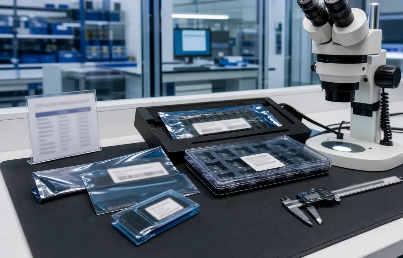
Model text, package form, tray or reel details, and visual evidence are reviewed together before RFQ feedback.
 WMSIC
Electronic Components
WMSIC
Electronic Components
Available for RFQ
Technical data
For datasheets, package documents, compatible-part guidance, or other technical resources, contact WMSIC customer service. Availability is confirmed case by case.
1SS272 (TE85L,F) 是东芝(TOSHIBA)面向小信号高速开关与精密整流场景推出的开关二极管器件。器件采用 SC-61B 小外形封装,内部为“2对串联式”结构,适合空间受限、对开关速度和反向漏电要求较高的便携与消费电子产品。其主要电气参数(在典型测试条件下)包括:正向压降 Vf = 0.920 V @ 100 mA、直流反向耐压 Vr = 80 V、整流电流 100 mA、耗散功率 Pd = 150 mW、反向电流 Ir = 500 nA @ 80 V、反向恢复时间 Trr = 1.6 ns、非重复峰值浪涌电流 Ifsm = 2 A。
器件采用 SC-61B 小体积封装,体积小、适合贴片工艺,但热阻相对较高,耗散功率 Pd = 150 mW 为整片器件(封装)允许的最大耗散。因该型号内部为“2对串联式”配置时需注意功耗分布:若电流经过两只串联二极管,则总正向压降为约 2 × 0.92 V = 1.84 V,对应在 100 mA 下的总功耗约 184 mW,已超过 Pd(150 mW),长时间工作会超出封装散热能力。推荐采取下列做法:
1SS272 (TE85L,F) 集低正向压降、低漏电、高耐压与极短反向恢复时间于小体积封装,适合高频开关、小信号整流及受限空间下的电子设计。设计时需注意封装耗散功率限制与内部串联结构对持续电流能力的影响,通过合理的 PCB 散热布局与电流限制措施,可在便携与消费电子产品中发挥其优良的高速与低漏电特性。若有更严格的热、脉冲或频率要求,建议参考完整的东芝器件规格书并与替代封装或更高额定器件进行比较选型。
Request for quote
Use the form for single models, category sourcing, and multi-line BOM requirements.
Product sourcing intelligence
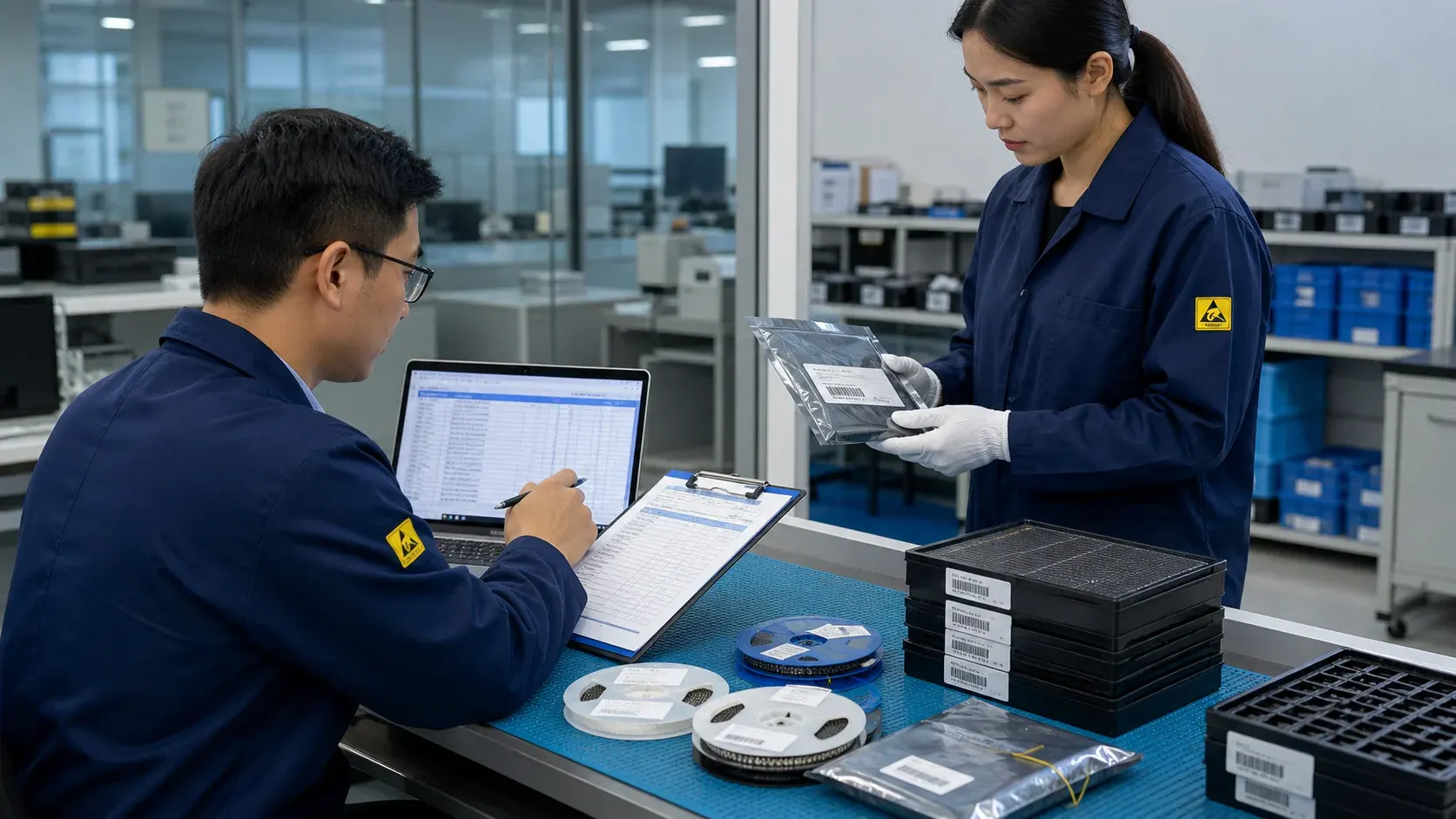
WMSIC turns product data, package visuals, BOM context, and sourcing signals into practical RFQ notes for buyers.
Model text, package form, tray or reel details, and visual evidence are reviewed together before RFQ feedback.
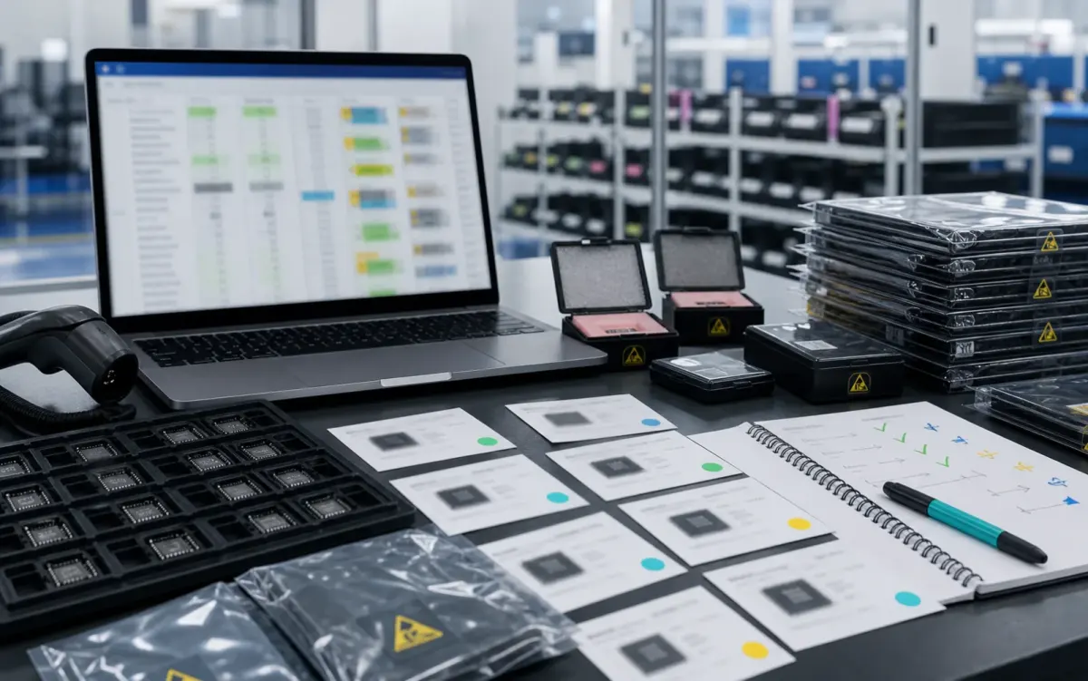
BOM lines are compared by package, parameters, quantity, and workable alternatives for cleaner sourcing decisions.
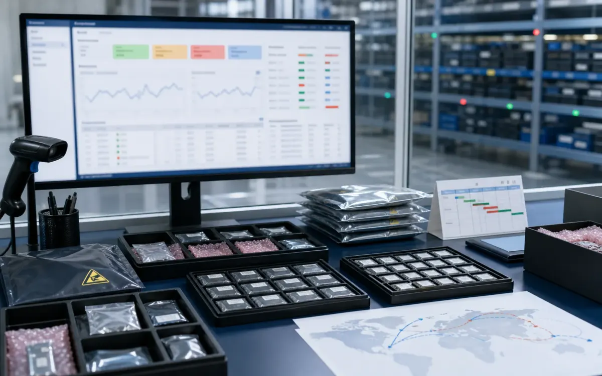
Stock routes, quotation confidence, lead-time notes, and shipment feasibility are checked before sales follow-up.
Buyer sourcing scenarios
Typical RFQ scenarios based on the WMSIC form fields, catalog data, manual review steps, and shipment preparation workflow.
The buyer shares the full part number, package requirement, quantity, destination, and available product photos so the quotation can record the exact version under review.
A multi-line BOM is organized into direct sourcing lines, lines that need package clarification, and lines where alternative-part review is permitted.
The original manufacturer part number, datasheet revision, application, critical limits, and acceptable changes are collected before possible candidates are discussed.
Sample quantity, minimum packing, package format, target date, and courier destination are kept together in one RFQ conversation.
Package photos, model markings, board context, and the quantity needed for repair help focus the sourcing review on the relevant version.
When a suffix or package note is incomplete, the response records the open difference and requests buyer confirmation before procurement proceeds.
Packing format, carton notes, invoice details, courier option, destination, and tracking handoff are coordinated around the confirmed order.
The request connects the previously used model, current demand, package evidence, target timing, and replenishment sourcing route.
Related products