Model & package intelligence
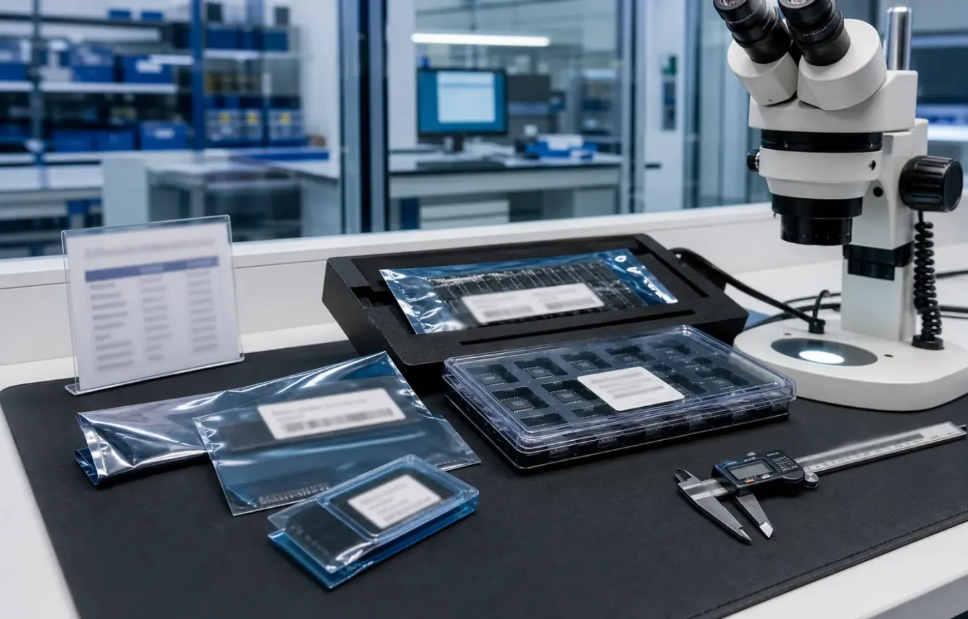
Model text, package form, tray or reel details, and visual evidence are reviewed together before RFQ feedback.
 WMSIC
Electronic Components
WMSIC
Electronic Components
Available for RFQ
Technical data
For datasheets, package documents, compatible-part guidance, or other technical resources, contact WMSIC customer service. Availability is confirmed case by case.
RN1426(TE85L,F)是一款针对小信号放大与数字逻辑驱动优化的晶体管,其关键参数可分为集电极-发射极、直流增益、输入特性三类,具体如下:
直流电流增益(hFE):90(测试条件:Ic=100mA、Vce=1V),该值在小信号放大场景下稳定,可有效提升输入信号的驱动能力,减少后续电路的负载压力。
该器件由东芝(TOSHIBA) 生产,品牌可靠性经过工业与消费电子领域长期验证,适用于对质量要求较高的场景。
封装形式为SC-59,属于超小型表面贴装封装(尺寸约2.9×1.6×1.1mm),具备三大优势:
RN1426(TE85L,F)的设计围绕小信号放大、数字逻辑匹配展开,核心特性包括:
VI(on)=2.5V、VI(off)=800mV的参数,完美适配常见的3.3V/5V数字逻辑电平(如MCU、FPGA输出),无需额外添加电平转换电路,简化系统设计流程。
在典型工作点(Ic=100mA)下hFE=90,确保小信号(如传感器输出的mV级信号)放大时失真小,信号传输质量稳定,适合对信号精度要求较高的场景。
Vebo=5V、Vceo=50V的击穿电压,配合内置1kΩ输入电阻,可有效抑制瞬态过压(如静电放电、电源浪涌),提升器件可靠性,减少故障概率。
Pd=200mW的耗散功率,结合SC-59小型封装,适合电池供电设备(如智能手表、无线耳机),延长续航时间。
基于上述特性,RN1426(TE85L,F)广泛应用于以下领域:
为确保器件稳定工作,需注意以下要点:
RN1426(TE85L,F)凭借小体积、稳定增益、电平匹配性、低功耗等优势,成为数字逻辑电路与小信号放大场景的高性价比选择,适用于消费电子、工业控制、通信模块等多领域,是设计紧凑、低功耗电路的理想器件。
Request for quote
Use the form for single models, category sourcing, and multi-line BOM requirements.
Product sourcing intelligence
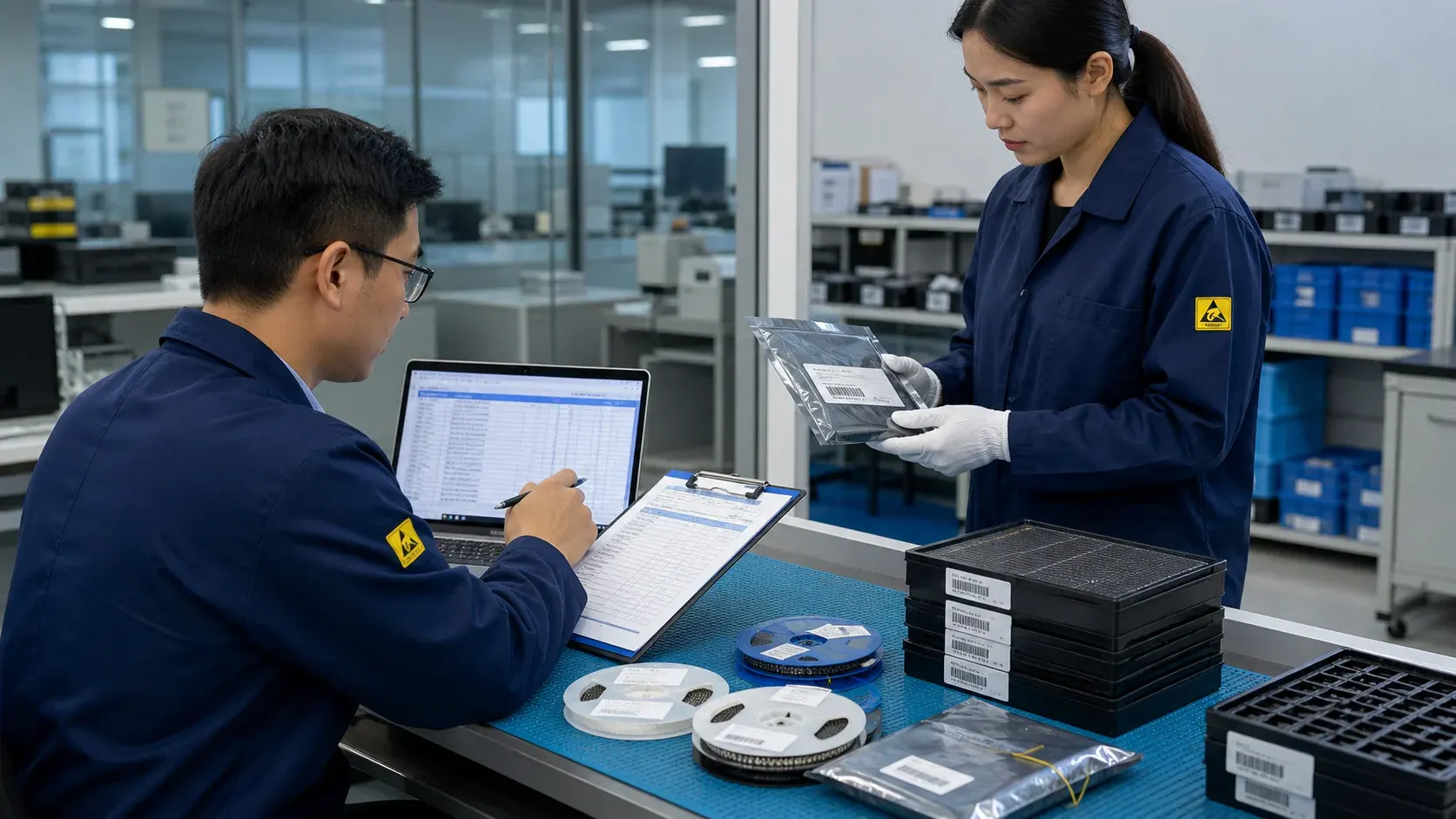
WMSIC turns product data, package visuals, BOM context, and sourcing signals into practical RFQ notes for buyers.
Model text, package form, tray or reel details, and visual evidence are reviewed together before RFQ feedback.
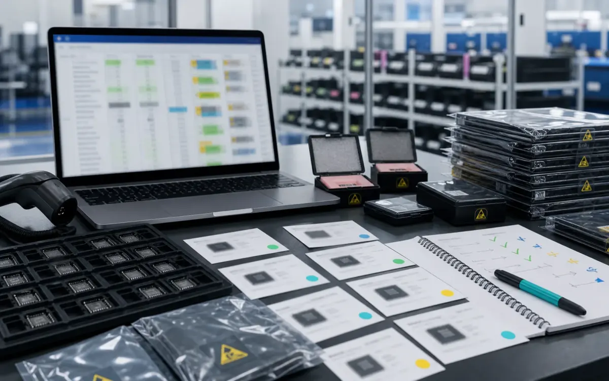
BOM lines are compared by package, parameters, quantity, and workable alternatives for cleaner sourcing decisions.
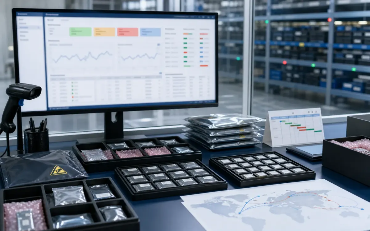
Stock routes, quotation confidence, lead-time notes, and shipment feasibility are checked before sales follow-up.
Buyer sourcing scenarios
Typical RFQ scenarios based on the WMSIC form fields, catalog data, manual review steps, and shipment preparation workflow.
The buyer shares the full part number, package requirement, quantity, destination, and available product photos so the quotation can record the exact version under review.
A multi-line BOM is organized into direct sourcing lines, lines that need package clarification, and lines where alternative-part review is permitted.
The original manufacturer part number, datasheet revision, application, critical limits, and acceptable changes are collected before possible candidates are discussed.
Sample quantity, minimum packing, package format, target date, and courier destination are kept together in one RFQ conversation.
Package photos, model markings, board context, and the quantity needed for repair help focus the sourcing review on the relevant version.
When a suffix or package note is incomplete, the response records the open difference and requests buyer confirmation before procurement proceeds.
Packing format, carton notes, invoice details, courier option, destination, and tracking handoff are coordinated around the confirmed order.
The request connects the previously used model, current demand, package evidence, target timing, and replenishment sourcing route.
Related products